
Flip chip mounts a die face-down onto a substrate using solder bumps or copper pillars. Area-array connections shorten paths versus wires to cut inductance and boost I/O density. Underfill epoxy controls CTE-driven stress and improves joint reliability. Fine-pitch builds use thermo-compression with non-conductive paste or film, plus molded or capillary underfill.
The short, wide interconnects lower power noise and give a better heat path. That enables high current and bandwidth in CPUs, GPUs, HBM, and FCBGA modules. At sub-10 µm pitches, microbumps hit limits and copper hybrid bonding takes over for more density. In the latest designs, flip chip packaging is the workhorse interconnect that makes the above practical.
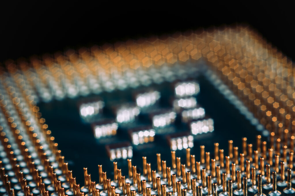
Flip Chip Package Structure and Its Key Components
Semiconductor Chip (Die)
The die is silicon with aluminum or copper bond pads opened through passivation. Pads get an under-bump metallization stack to wet solder, block diffusion, and spread current. Redistribution layers can move pads into an area array for dense I/O. It sets the pad size and reliability limits.
Conductive Bumps
Lead-free solder bumps (for example, tin–silver–copper alloys) remain common for cost and throughput. Copper pillars add fixed standoff, finer pitch, and better current handling at advanced nodes. Adhesive routes exist, too. Anisotropic conductive films and isotropic conductive adhesives can be utilized at lower heat, along with tradeoffs in resistivity and aging. Remember, process windows and reliability differ sharply across these choices.
Substrate or Interposer
Organic substrates (BT/ABF) dominate for cost and routing density. Ceramics (AlN, LTCC) serve high-frequency and hot parts thanks to stiffness and thermal conductivity. Meanwhile, silicon interposers enable 2.5D links like HBM. Glass cores offer very low loss and tunable CTE with through-glass vias. Silicon also supports MEMS and silicon-photonics co-packaging. Such choices drive signal integrity, warpage, and cost in flip chip packaging.
Underfill Material
Underfill is an epoxy that wicks by capillarity under the die and cures to redistribute CTE-mismatch stress. Adhesion, modulus, coefficient of thermal expansion, and Tg largely set joint fatigue life. Variants include capillary, no-flow, and molded underfill, depending on pitch and throughput. It is central to mechanical strength in flip chip packaging.
Encapsulation
Mold compounds or glob-top resins add environmental protection against shock, moisture, and contamination. EMC properties also affect package warpage and moisture sensitivity class, so filler, modulus, and Tg matter. Good moisture control avoids popcorning and delamination at reflow. In flip chip packaging, EMC selection must meet the underfill and substrate stack.
Flip Chip Assembly Process
- Chip Preparation and Bump Formation: Wafers open pad windows, add under-bump metallization, and build bumps by plating. Copper pillars grow on a Cu seed with photoresist defining height and diameter. A Ni barrier under a Sn-Ag cap limits brittle intermetallics. Micro-bump chemistry and plating rates set pitch and standoff. Ultimately, these steps set the I/O density and planarity for flip chip assembly.
- Substrate Preparation (Fluxing): Pads use finishes like ENEPIG or EPIG. Flux is applied by dip, pin transfer, or stencil print for wetting. Jetting and spray methods exist for very fine pitches. Formic-acid reflow enables fluxless soldering when residues are a risk. Method choice depends on pad finish, oxidation, and pitch.
- Precise Die Placement and Alignment: Flip-chip bonders place the die within a few microns. During reflow, surface tension self-centers the die and corrects small offsets. With non-conductive paste or film, thermo-compression bonding adds heat and force for wetting and curing. Tight placement matters as bump pitch shrinks.
- Reflow Soldering for Electrical/Mechanical Connection: Controlled profiles melt the solder, wet the under-bump metallization and pads, and form intermetallics. Nitrogen or formic-acid atmospheres reduce oxidation and improve wetting. Surface tension completes fine alignment during the liquid phase. For the tiniest spacing, we may press/heat each part with the underfill already there, instead of baking everything at once.
- Underfill Dispensing and Curing: Capillary underfill wicks from die edges and cures to redistribute CTE-mismatch stress. No-flow underfill co-cures during soldering to cut steps at fine pitch. Wafer-level or molded underfill options trade cycle time against void risk and rework. Voids and poor fillets are major reliability limiters.
- Testing and Inspection (Electrical, X-Ray): Daisy-chain tests screen opens and shorts. X-ray reveals bridges and voids under the die. C-SAM maps delamination at the die, underfill, and substrate interfaces. These checks close the flip chip assembly flow.
Flip Chip Technology: Key Factors in Performance, Materials, and Reliability
Performance Requirements
Evaluate signal integrity, power delivery, and thermal needs first. Flip chip’s short interconnect paths reduce loop inductance and voltage drop. Copper pillars support fine pitch and high current with better standoff control and lower parasitics. Before layout, model channel loss and power delivery impedance to confirm flip chip is the right choice.
Material Compatibility
Select materials based on operating conditions. Organic ABF cores work for dense routing, while ceramic AlN is better for high junction temperatures or low RF loss. Check CTE, Tg, Dk, and moisture resistance against your expected duty cycle. Validate solder alloy and underfill performance with thermal cycling data.
Manufacturing Capability
Assess your supplier’s process control and inspection standards. Review placement accuracy, reflow atmosphere, and readiness for TCB or NCF. Formic-acid reflow can enable fluxless joints and lower voiding. Require compliance with IPC-9701A board-level reliability and proper handling of moisture sensitivity levels. Ensure X-ray and C-SAM inspection coverage, and confirm proven yield at your target pitch.
Design Flexibility
Plan for future integration. Silicon interposers boost bandwidth and power density, while glass cores reduce loss and warpage in larger substrates. Check supply chain capacity for interposer availability and panel size. Flip chip technology is often preferred when scaling to 2.5D/3D integration or co-packaged optics.
Partner with FICG for Advanced Flip Chip Solutions
FICG combines deep expertise in flip chip technology, proven high-volume manufacturing capabilities, and a future-proof R&D roadmap. Whether you need high-density interconnects, advanced silicon photonics integration, or co-development of new packaging solutions with customers, our engineering teams are ready to support your next-generation products with reliable, high-performance solutions.