Bandwidth is rising. So are thermal constraints, component counts, and performance demands in everything from AI servers to metro switches. As optical module design pushes for tighter layouts and lower parasitics, Surface Mount Technology (SMT) becomes a foundational manufacturing choice. SMT shortens interconnect paths, supports dense multi-layer PCBs, and streamlines high-volume builds—all critical in optical communications.
FICG’s SMT capabilities are purpose-built for this new environment. With automated lines tuned for component accuracy, thermal balance, and signal integrity, our SMT platform supports everything from small-form-factor transceivers to high-speed, co-packaged optics. Here’s how the process works, how to pick the right SMT type, and why our model delivers consistent high-yield performance.
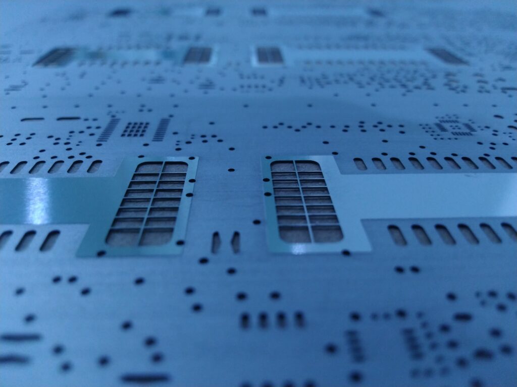
How Does Surface Mount Technology Work?
Solder Paste Application
It starts with stencil printing. A mix of solder alloy and flux is applied to precise PCB pads using automated stencil printers. Paste volume and pad alignment are critical here—especially for 0.5 mm fine pitch. At FICG, our lines support down to 0.1 mm fine pitch, reflecting our ability to handle today’s smallest solder ball and spacing requirements for advanced optical modules.
Component Placement
Next, SMDs are mounted by pick-and-place machines. FICG’s high-speed lines support 0.25mm pitch IC packages and BGAs with ±10µm placement accuracy. This ensures stable yields even in the extreme layouts of high-speed optical modules and AI accelerator boards, where density and precision are critical.
Reflow Soldering
Boards pass through reflow ovens, where temperature profiles are tuned per board stack-up and paste type. The paste melts, wets the component leads, and forms solid solder joints. FICG’s convection systems support tightly controlled ramp rates and multi-zone heating—ensuring reliable solder joints on critical optical interfaces.
Inspection and Testing
Every PCB faces AOI (Automated Optical Inspection) for component alignment and solder joint quality. Complex packages or hidden joints go through 3D X-ray, including CT function. Final tests simulate real-world workloads. FICG ties all results to MES systems, so traceability runs back to the individual reel and lot.
Insight: According to IPC standards, consistent solder quality and traceability are essential in high-reliability applications like telecom, aerospace, and data communications.
Types of SMT and Their Applications
Type I SMT – Pure Surface Mount Assembly
- Uses SMDs on one or both PCB sides.
- Ideal for low-to-medium complexity boards.
- Best fit for compact designs needing cost and space efficiency.
Type II SMT – Mixed Technology Assembly
- Blends SMT and through-hole components on the same side.
- Through-hole parts add mechanical strength (e.g., connectors, coils).
- Used when designs require electrical density plus robustness.
Type III SMT – Mixed Technology with Component Split
- Maximizes PCB real estate and structural durability.
- Typical in telecom backplanes or power-sensitive optical drivers.
How to Choose the Right SMT Assembly Type

Circuit Complexity
High-density signal processing or optical routing often needs dual-sided SMT. That’s where Type I or II comes in. For simpler logic or control boards, single-sided Type I is enough.
Component Requirements
If your module has optical cages, RF connectors, or heavy inductors—Type II or III offers better mechanical strength due to through-hole mounting.
Cost Efficiency
Type I gives lean manufacturing and low BOM. It’s the go-to for pluggable modules or evaluation boards. Type II and III are better when long-term reliability outweighs part count.
FICG’s Competitive Edge in SMT
End-to-End Automation
Our lines integrate stencil printing, component placement, reflow, inspection, and inline testing. This vertical integration means fewer variables, faster feedback loops, and better control over thermal profiles and component stress.
High-Precision Placement
At FICG, we routinely place 008004, 01005, and 0201 miniature passives with exceptionally high yield. We achieved mass production certification for 008004 packages as early as 2017, proving our long-standing capability in fine-pitch assembly. Today, our SMT platform supports 0.25 mm pitch high-speed IC packages and fine-pitch BGAs.
In volume runs, first-pass yields reach 99.997% (30 dppm) for 01005 packages and 99.999% (10 dppm) for 0201 packages. This level of precision ensures stable quality and consistent signal integrity, even in the demanding layouts of high-speed optical modules, AI high-speed boards, and 5G networking equipment. Multiple SPI and AOI checkpoints further reduce solder paste printing, placement defects and rework across both NPI and mass production, making the process highly predictable and controlled.
Zero-Defect Mindset
Every solder joint is inspected, either optically or with X-ray, to ensure quality at the source. Functional testing then validates performance under real operating loads. All results are tied into our MES system, linking data back to serial number, operator, and lot. This closed-loop approach strengthens traceability, minimizes defects, and maintains consistent reliability across complex optical PCBs.
Production Volume
FICG’s SMT lines run 24/7 with cycle times optimized for mid- to high-volume production. This setup ensures predictable, consistent results at scale, giving optical module customers reliable capacity without compromising quality.
Thermal and Signal Integrity Optimization
Our process engineers fine-tune paste type, reflow profiles, and pad design for each layout. On optical and AI boards, we optimize via-in-pad layouts and ground return paths to minimize jitter and maximize thermal headroom. Careful control of stencil design and solder volume also reduces risks such as tombstoning, improving overall yield and cutting debug time during both NPI and mass production.
Build Smarter, Faster, and More Reliable with FICG SMT
Surface Mount Technology underpins every high-speed, high-density electronic product today—from compact transceivers to 3.2T, co-packaged optics. The right SMT type ensures your PCBs meet cost, performance, and durability goals. FICG’s manufacturing ecosystem combines precision placement, zero-defect inspection, and signal-aware layout guidance to deliver PCBA platforms optimized for optical communications, AI servers, and advanced networking. FICG combines cutting-edge SMT manufacturing technology with deep domain expertise in optical communications, enabling robust, high-performance PCBA solutions tailored for next-gen data centers, 5G, and AI workloads.
Contact us to discover how our SMT capabilities can power your innovative optical modules with unmatched quality and efficiency.